FINAL YEAR DESIGN PROJECTS OF
MECHANICAL ENGINEERING
2006/2007
Design and Fabrication of a Micro
Biometric Sensor – Fingerprint Sensor to Enhance the Security of Portable
Electronics
Group size:
5 students
Supervisor: Prof. Yi-Kuen Lee
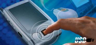
Micro biometric sensors are becoming more and more important for the security of portable electronic devices, such as laptop computers, PDAs and mobile phones because these devices can either store or transfer huge amount of personal information in very short period of time. Since the conventional security measure using “password” can be easily cracked, many large IT companies are trying new methods to enhance the security of their products, such as IBM thinkpad T43 computers, HP Compaq NX6125, etc. It is estimated that with an average annual growth rate of 29.1%, the world biometric market would reach $3.4 billion by 2007. This will predominantly include fingerprint scan technology (59.4%), facial and iris scanning (13%), keystroke (0.4%) and signature scans (2.7%). In particular, the biggest market of fingerprint sensors is in the security enhancement of portable electronics (International Biometric Group).
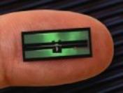
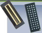
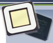
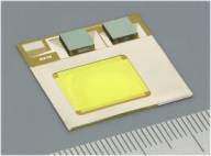
This FYDP project is to design, manufacture and test a micro pressure-type fingerprint sensor. The design project includes five tasks: 1) Design and fabrication of a pressure-type micro fingerprint sensor, 2) Performance and reliability testing of fingerprint sensors, 3) Design and fabrication of the interface electronics for the fingerprint sensor to the portable electronics, 4) System integration and packaging of micro fingerprint sensors, 5) Self-cleaning coating on the surface of micro fingerprint sensors.
The design and manufacturing of the prototype fingerprint sensor chip are challenging. Students will go through training of basic MEMS design and analysis, hands-on micro-fabrication in the world-class clean room (www.mff.ust.hk), packaging and testing of the microchip in this project. Both team work and individual efforts will be emphasized. Each student will be responsible for one of the following design and manufacturing:
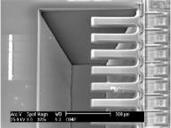
1. Design and Fabrication of a Pressure-type Micro Fingerprint Sensor
Design objectives: design a simple and economic micro
fabrication process to realize a micro fingerprint sensor with high resolution
and lost cost,
2. Performance and Reliability Testing of Micro Fingerprint Sensor
Design objectives: design an experimental setup to evaluate the
performance and reliability of the fabricated fingerprint sensor,
3. Design and Fabrication of the Interface Electronics for the Micro Fingerprint Sensor to the Portable Electronics
Design objectives: design the interface electronic circuit
and/or software for the fingerprint sensor to be used in portable electronic
devices,
4. Packaging of Micro Fingerprint Sensor and Integration to the Portable Electronics
Design objectives: design
the cost-effective packaging solution for the micro fingerprint sensor,
5. Self-Cleaning Coating on the surface of Micro Fingerprint Sensor
Design objectives: design
the surface coating process to enhance the reliability of micro fingerprint
sensor.
-
Prof Yi-Kuen
Lee
-
Dr LU Miao
-
WAN Kwok
Leung me_wklab @ ust.hk (Team Leader)
-
AU Hin
Liang me_ahl @ust.hk
-
CHOW Ping
Chuen me_cpc @ust.hk
-
LO Kai Kin me_lkkab @ust.hk
-
SO Wai
Chung me_swc @ust.hk
Collaboration:
-
Prof Amine Bermak in ECE Dept of
HKUST
-
PhD student:
Guo Bin, guobin@ust.hk
1. Human
fingerprint characteristics
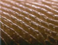
Under normal condition, the ridges and valleys, are 300~500 mm wide and 50~100 mm deep. The elastic modulus of tissue is about 20 GPa. Dielectric constant is about 45 at 1~3 GHz. The resistance and capacitance of tissue will change with different frequency as showed in following diagram. From: Human tissues at 37ºC (Cook, 1952).
2. Fingerprint sensor chip physics
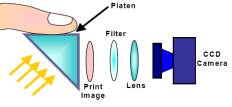
2.1 Optical readers
The oldest 'live-scan' readers use frustrated refraction over a glass prism (when the skin touches the glass, the light is not reflected but absorbed). The finger is illuminated from one side with a LED while the other side transmits the image through a lens to a camera.
Optical FPS can also work on scan/sweep mode.
2.2 Electro-optical readers
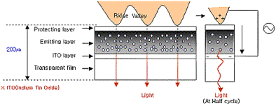
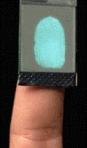
Some polymers are able to emit light when properly excited with the proper voltage (generally quite a high voltage is required. This polymer is directly contacting a CMOS camera, which is necessarily the size of the finger. Generally, the finger acts as the ground, and the polymer emits light where the ridges touch.
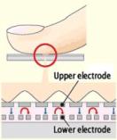
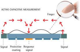
2.3 Capacitance Reader
2.3.1 Silicon chips + capacitance
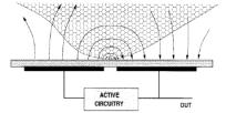
2.3.2 Capacitance + TFT
Flat panel technology rather than bulk silicon has been studied by Philips Korea and some others using capacitive sensing.
Reference:
- http://perso.orange.fr/fingerchip/biometrics/types/fingerprint_sensors_physics.htm
- A Capacitive Fingerprint Sensor with Low-Temperature Poly-Si TFTs Mitsubishi Electric Corp.
- (April 2004) Alps Electric develops 2 fingerprint sensors. One is transparent, electrostatic (capacitive).
2.3.3 RF field - AC capacitance
Low radio frequency (RF) signal is injected into the finger, then read by the pixels on the silicon acting like antennas. The signal strength depends on the capacitance, so from the distance between the skin and the pixel.
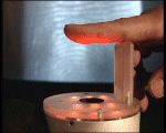
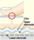
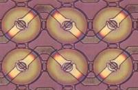
2.4 Pressure Reader
This is one of the oldest ideas, because when you put your finger on something, you apply a pressure. Piezoelectric material has existed for years, but unfortunately, the sensitivity is very low. Moreover, when you add a protective coating, the resulting image is blurred because the relief of the fingerprint is smoothed.
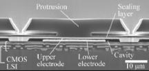
2.4.1 Conductive membrane on a CMOS silicon chip/TFT
Reference:
- http://perso.orange.fr/fingerchip/biometrics/types/fingerprint_sensors_physics.htm
- Opsis
(a french company) offered a device using a conductive membrane
deposited on a CMOS chip (July 1994).
- Since
2002, BMF
is offering a product using a TFT substrate (developed with Sanyo)
- Fidelica offers since mid-2004 the FIS-3002, also using a TFT substrate from Sanyo

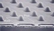
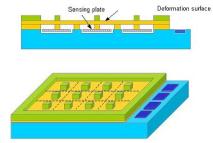
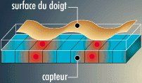
2.4.2 Tactile MEMS reader
Micro electro-mechanical devices allow engineers to make extremely tiny silicon switches. When a ridge touches a switch, it closes. But the coating remains a significant problem, and moreover, a binary image is the result, leading to minimal information. No further development has been done with this technique beyond the laboratory.
· NTT research group · NTT Microsystem Integration Laboratories
Michigan University (Wise) Tima homepage
Leti, pressure sensors (Rey) LighTuning
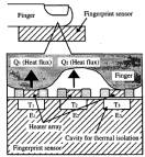
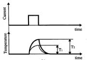
2.5 Thermal Reader
Pyro-electric material is able to convert changes in temperature into a specific voltage. This effect is quite large, and is used in infrared cameras. This type of sensor doesn't measure the difference of temperature between the skin in the ridges and valleys, because the difference is negligible. In fact, as the finger is directly placed on the material, the ridge's temperature is what's measured, as it's in contact. The valleys don't make contact, so the temperature of the pyro-electric material under the valleys remains almost unchanged. A drawback of the technique is that the image disappears quickly. When you place your finger on the sensor, there is a big change of temperature, and therefore signal, but after a short period (less than a tenth of a second), the image vanishes. The finger and the chip have reached thermal equilibrium, and as there is no change in temperature, there is no signal. This effect disappears when you sweep your finger over the sensor, because of the touch/no touch of ridge/valley.
Reference:
- http://perso.orange.fr/fingerchip/biometrics/types/fingerprint_sensors_physics.htm
- Atmel (formerly Thomson-CSF) proposes the FingerChip
- Hunno Technologies & Hyosung Corp and Hyung-Kew Lee (Korea, KAIST) have studied a thermal fingerprint sensor in 1999, probably using bolometers.
- Nagoya University
has studied a thermal sensor based on MEMS, using a resistor to heat a
sensor above a cavity.
INO ( Canada) has used bolometers to make a 160x120 pixel fingerprint sensor (US patent 6,633,656). Bolometric FPA for fingerprint recording - IMTEK & Schippers propose a fingerprint sensor based on a similar technique as Nagoya Univ., adapted for a smart card.
- BMF Inc, Kanagawa, Japan (Biometric Fingerprint Sensor) BLP-100 is the world's first pressure sensitive fingerprint sensor. Unlike other sensors in the market, it allows you to clearly sense both dry and wet fingers
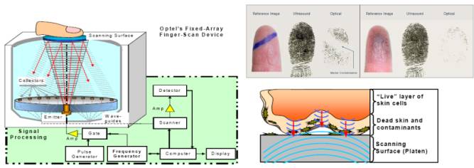
2.6 Ultrasonic Reader
Ultrasonic sensing requires quite a big device with mechanical parts, and is quite expensive. Moreover, it takes a few seconds to grab an image. It is not suited for large production volumes at low cost. Its main advantage is the reading of the derma, the sub-surface of the skin, rather than the surface.
· Optel is still at R & D stage.
3 Fingerprint sensor system and
packaging
A fingerprint sensor is a complex system. First, the output analog signal of the sensor array must be balanced, amplified, and changed to serial or parallel digital signal (data). Secondly, a certain of algorithm stored in CPU or DSP compare these data with initial data in memory.
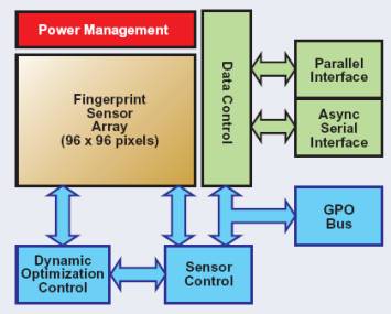
Some latest packaging technology including BGA, HDP and Flip clip, are applied in the packaging of fingerprint. Additionally, some special coatings on the surface of the sensor are needed to make the sensor durable and avoid grease or sweat contamination.
4.
Algorithms
Algorithms
are usually using a combination of these following techniques:
·
Most algorithms are using minutiae, the specific points like ridges
ending, bifurcation... Only the position and direction of these features are
stored in the signature for further comparison.
·
Some algorithms counts the number of ridges between particular points,
generally the minutiae, instead of the distances computed from the position.
·
Pattern matching algorithms are using the general shape of the ridges.
The fingerprint is divided in small sectors, and the ridge direction, phase and
pitch are extracted and stored.
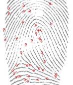
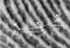
minutiae in
fingerprint ridge
count algorithm
5.
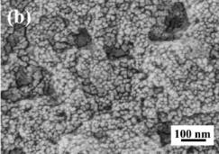
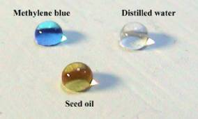
Hydrophobic self-cleaning Coating
The
self-cleaning action of hydrophobic coatings stems from their high water &
oil contact angles; water & oil on these surfaces forms almost spherical
droplets that readily roll away carrying dust and dirt with them. Dirty water
falling onto the hydrophobic coating is removed before it can evaporate.